Modular Systems > National Instruments > R Series


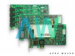
Pictures shown are a representation. Actual item may vary if no part number is provided on quote request.
✔ Same Day Calibration Available
✔ 2-3 Year Warranty Included
✔ Free Ground Shipping
Or speak to a sales representative for additional information:
Phone:
1-800-915-6216Email:
sales@apexwaves.comPCIe-7841 Request for Availability
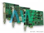
PCIe-7841, 96 DIO, Virtex-5 LX30 FPGA, Multifunction Reconfigurable I/O Device
National Instruments PCIe-7841 Multifunction Reconfigurable I/O Device
The PCIe-7841 is a Multifunction Reconfigurable I/O Device manufactured by NI. The part number of the NI PCIe-7841 is 781100-01. This device supports individual channel triggering and sampling at different rates. This model can be used to control signals. The PCIe-7841 has an onboard FPGA. The FPGA type is Virtex-5 LX30. The FPGA controls signal processing and provides flexible timing and synchronization for the system. Independent timing and triggering are also supported by the PCIe 7841. A dedicated ADC is incorporated for this purpose.
The NI PCIe-7841 Multifunction Reconfigurable I/O Device has eight analog input terminals, which can be used in three different modes: DIFF, RSE, and NRSE. The desired mode is selected through software. These terminals support an input signal in the range of +10 V, can sample data at a maximum rate of 200 kS/s, and have a resolution of 16 bits. The input terminals have the impedance of 10 GΩ. It is equipped with 3 68-pin female high-density VHDCI I/O connectors.
The PCIe-7841 also features eight single-ended analog output terminals. These terminals have a maximum update rate of 1 MS/s. The impedance of the output channels of this device is 0.5 Ω. The analog terminals are DC-coupled and have a resolution of 16 bits. The PCIe 7841 offers overvoltage protection for the analog terminals; they can sustain up to +42V. The output terminal’s protection is the short circuit to ground.
The NI PCIe-7841 Multifunction Reconfigurable I/O Device comes with 96 digital I/O terminals, and 3 DMA channels. These digital terminals are TTL compatible. The digital terminals of the device support two logic levels: 3.3 V and 5V. The output current of the digital terminals is 4.0 mA. The digital terminals can sustain an overvoltage of +20 V without getting damaged.
The NI device weighs 0.28 lb, and measures 6.7 x 4.3 in. in physical dimensions. It has a recommended operating temperature range of 0 °C to 40 °C, a storage temperature range of –20 °C to 70 °C, and a non-condensing operating and storage humidity range of 10% to 90% and 5% to 95% respectively.
| Model | PCIe-7841 |
|---|---|
| Manufacturer | National Instruments |
| Series | R Series |
| Part Number | 781100-01 |
| Type | Multifunction Reconfigurable I/O Module |
| FPGA Type | Virtex-5 LX30 |
| Analog Inputs | 8 (16 Bits, 200 kS/s) |
| Analog Outputs | 8 (16 Bits, 1 MS/s) |
| Number of Flip-flops | 19,200 |
| Number of 25 × 18 Multipliers | 32 |
| Embedded Block RAM | 1,152 kbits |
| Digital I/O | 96 |
| Number of DMA Channels | 3 |
| Timebase | 40, 80, 120, 160, or 200 MHz |
| I/O Connectors | 3 × 68-pin Female High-Density VHDCI |
| Power Requirements | +3.3 VDC, 12 VDC - 847 mA, 0.5 A |
| Dimensions | 6.7 in. × 4.3 in. |
| Weight | 0.28 lb. |
| Software Driver | NI-RIO |
| Warranty | Three Year Warranty |
| PCIe-7841 Manual | User Manual and Maintenance Manual Available for Download |
| Price | Contact a sales representative for a quote. |
Associated part numbers for PCIe-7841:
National Instruments PCIe-7841 Frequently Asked Questions
Question: Is it possible to use a PCIe-7841 with NI-DAQmx for analog input and output?
Answer: The PCIe-7841 does not work with NI- DAQmx, it requires a LabVIEW FPGA.
Question: What is the clock rate of the PCIe-7841?
Answer: The clock rate of the PCIe-7841 is 40MHz.
Question: How do I output a voltage via one of the analog outputs for the NI PCIe-7841?
Answer: To output a voltage via the analog output for the NI PCIe-7841, do a LabVIEW to FPGA interface using C interface to LabVIEW FPGA. Once you deploy your code to FPGA and write your C code and then create a .dll out of your C code.
PCIe-7841 PDF Manuals
GETTING-STARTED-WITH-R-SERIES-MULTIFUNCTION-RIO.PDF
NI-78XXR-PINOUT-LABELS-FOR-THE-SCB-68-NOTE-TO-USERS.PDF
NI-78XXR-PINOUT-LABELS-FOR-THE-SCB-68A-NOTE-TO-USERS.PDF
NI-R-SERIES-CALIBRATION-PROCEDURE.PDF
NI-R-SERIES-INTELLIGENT-DAQ-USER-MANUAL.PDF
NI-R-SERIES-MULTIFUNCTION-RIO-SPECIFICATIONS.PDF
Delivery:
Warranty:
All of our products are covered by our Apex Waves Warranty.
✓ 3 Year Warranty - New Surplus Parts
✓ 2 Year Warranty - Refurbished Parts
Returns:
No hassle return policy.
Dedicated customer service team.
Payment:


Quick Quotes:
Receive Price & Availability Today!
Calibration:
Ask About Our Tiered Calibration Levels
Option & Modules:
Confirm Your Requirements or Versions
Repair:
Cost & Lead Time Available Upon Request for Service
Repair Evaluation: $150
Common Typos: