Semiconductors, the tiny powerhouses at the core of our modern electronics, undergo a rigorous journey before they make their way into our devices. The testing process in semiconductor design is vital, ensuring that these minuscule components meet the highest quality standards. In this blog post, we’ll take you step-by-step through the semiconductor testing process and discuss why it’s absolutely crucial.

What are the Types of Testing in the Semiconductor Industry?
1) Wafer-Level Testing:
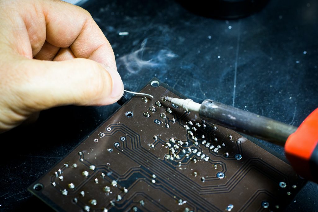
Probe Testing: The journey begins with the silicon wafer. Probe testing, also known as “wafer sort,” involves making electrical contact with individual devices on the wafer. It serves as the initial check for basic functionality, identifying and excluding defective devices early in the manufacturing process.
2) Package-Level Testing:
•••••• Final Test: After devices are cut from the wafer and packaged into their final form, they undergo final testing. Electrical signals are applied to assess the device’s performance under various conditions.
•••••• Functional Testing: This stage evaluates whether the device performs its intended functions, running test programs to ensure correct execution of instructions.
•••••• Parametric Testing: Specific electrical parameters are measured to ensure they fall within specified ranges.
•••••• Speed and Timing Testing: For devices with clock frequencies or timing requirements, this checks if the device can operate at specified speeds and meet timing constraints.
•••••• Power Consumption Testing: Measures power consumption under different operating conditions to ensure power efficiency.
3) Environmental Testing:
•••••• Temperature Testing: Devices undergo testing at extreme temperatures to evaluate performance under varying thermal conditions.
•••••• Humidity Testing: Some devices are subjected to humidity testing to assess their resistance to moisture-induced failures, particularly relevant in harsh environments.
4) Reliability Testing:
•••••• Burn-In Testing: Devices may be operated at elevated temperatures for an extended period to identify and eliminate early-life failures caused by manufacturing defects.
•••••• Accelerated Life Testing (ALT): Simulates years of usage in a short time by subjecting devices to extreme conditions to predict reliability over the expected lifespan.
5) Custom Testing:
Depending on specific device requirements and applications, custom tests may be conducted to evaluate unique features or functionalities.
6) Data Analysis and Reporting:
The results from all testing stages are collected, analyzed, and documented. Any failures or deviations from specifications are noted, and decisions are made regarding device quality.
7) Marking and Packaging:
Once a semiconductor device passes all tests, it is marked, packaged, and prepared for distribution or integration into electronic systems.
NI’s Semiconductor Testing Solution
The NI Semiconductor Test System (STS) is a comprehensive and versatile platform designed specifically for semiconductor production testing. It is tailored to address the complex and high-throughput testing requirements of semiconductor manufacturing using modular architecture, high-performance measurement hardware, and test executive software.
Typical STS configurations can be scaled, and include hardware such as a Vector Signal Transceiver (ex: PXIe-5644), a Digital Pattern Instrument (ex: PXIe-6571), a Waveform Generator (ex: PCI-5402), an Oscilloscope (ex: PXI-5105), or a Sound and Vibration Instrument (ex: PCI-4472).
What is the Testing Process of Semiconductors?
Quality Assurance: Testing ensures that only high-quality semiconductor devices enter the market, preventing subpar components from compromising electronic systems’ reliability. Testing identifies defects early, reducing the likelihood of device failures and increasing their overall reliability.
Performance Validation: Testing verifies that devices meet their intended specifications, ensuring they perform as expected in real-world applications.
Customization: Custom tests allow for the evaluation of specialized features, meeting the diverse needs of various applications.
Cost Reduction: By identifying and addressing defects and optimizing processes, testing ultimately leads to cost savings, benefiting both manufacturers and consumers.
Environmental Testing: Ensures devices can withstand harsh conditions, making them suitable for diverse environments and applications.
Data-Driven Decision-Making: Test data guides improvements in design and manufacturing processes, enhancing the overall semiconductor production ecosystem.
In conclusion, the semiconductor testing process is a meticulous and essential journey that ensures the high quality, reliability, and performance of the devices powering our digital world. Without these tests, our electronic systems would be far less reliable, efficient, and safe. Test and measurement is important because it ensures that the semiconductors operate with precision and excellence.
Additional Information: